Introduction
Thin films are the unsung heroes of modern electronics. Found in everything from power modules to solid-state devices, they dissipate excess heat or channel it efficiently toward a heat sink. As devices shrink and power densities rise, the thermal conductivity of these films, often just tens of micrometers thick, has become a limiting factor in thermal management performance. Measuring it accurately, however, is easier said than done.
A study published in the ASME Journal of Heat and Mass Transfer introduces a novel transient plane source (TPS) approach that addresses one of the most persistent problems in thin film characterization: thermal contact resistance (TCR).
The Measurement Challenge
The conventional TPS method for thin films, typically applied to films and adhesives between 50 and 200 μm, requires no sensor deposition on the sample. But it suffers from a hidden weakness.
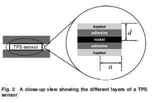
Thermal contact resistance arises between the sensor layers, between the sensor and the film, and between the film and the background material. These unwanted resistances add to the film's own thermal resistance, systematically producing conductivity readings that are too low.
Steady-state alternatives avoid some of these issues but demand long measurement times, careful calibration, and often micro-fabricated heaters deposited on the film itself.
Key Insights from the Study
The novel approach, validated against a guarded heat flow meter, rethinks the measurement configuration entirely:
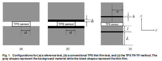
- One-dimensional heat flow: The sensor, background material, and thin film all share the same radius, forcing heat to flow in a single dimension.
- A decoupling slab: A thin slab of the same background material (stainless steel in this study) is inserted between the TPS sensor and the film. This physically separates the sensor from the film, decoupling the sensor's contact resistance from the film's thermal resistance, and eliminating the need for a separate reference test.
- Multiple thicknesses, linear regression: By testing stacks of one, two, and three identical film layers and regressing thermal resistance against thickness, the remaining contact resistances can be extracted from the slope and intercept of the fit.
- Speed: Each measurement takes only seconds, a stark contrast to the long equilibration times of steady-state methods.
The results speak for themselves. Four materials, a polyimide, a PTFE, a thin glass, and a graphite film, were measured with the new approach and cross-checked against a guarded heat flow meter. The agreement was excellent: differences below 12%, averaging around 5%. The study also confirms that a thermal contact agent between layers is strongly recommended to minimize microscopic surface roughness effects.
Beyond free-standing films, the method shows promise for multilayered structures, coatings, cured adhesives, and even the direct measurement of thermal contact resistance, an area that currently lacks suitable methodologies.
Selecting the Right Method, Not Just Any Method
This study reinforces a principle we hold dear: no single test method fits all materials. Thin films illustrate this perfectly, where an unsuitable method can distort results by more than the effect you are trying to measure.
That is why we assess thermal conductivity by the most suitable method for your application, whether that is (modified) TPS, heat flow meter (HFM), guarded hot plate (GHP), transient line source (TLS), laser flash analysis (LFA), or dedicated thermal interface material (TIM) testing.
Complementary properties such as thermal diffusivity and thermal Effusivity, alongside the full thermal analysis toolbox (DSC, TGA, TMA, DMA, and calorimetry), complete the picture.
Why Partner with EXPERTA | TESTING?
Whether you are developing next-generation thermal interface materials or qualifying films for electronic assemblies, we simplify material testing so you can focus on innovation.
Interested in thin film thermal characterization? Contact us via info@experta-testing.com.
EXPERTA | TESTING - Simplify Material Testing